- 您现在的位置:买卖IC网 > Sheet目录3851 > PIC32MX130F064D-I/ML (Microchip Technology)IC MCU 32BIT 64KB FLASH 44-QFN
PIC32MX1XX/2XX
DS61168D-page 14
Preliminary
2011-2012 Microchip Technology Inc.
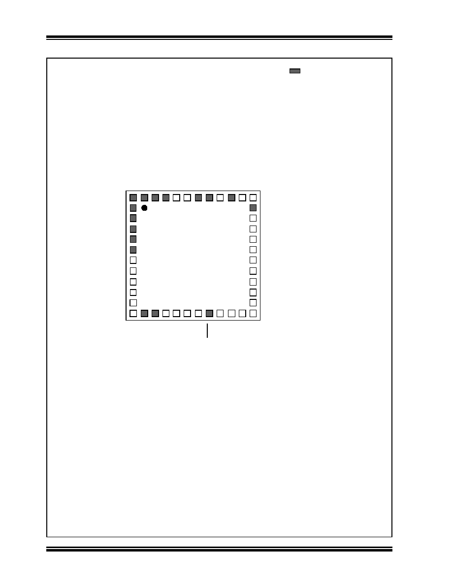
Pin Diagrams (Continued)
44-Pin VTLA(1,2,3)
= Pins are up to 5V tolerant
Note
1:
The RPn pins can be used by remappable peripherals. See Table 1 for the available peripherals and Section 11.3 “Peripheral
Pin Select” for restrictions.
2:
Every I/O port pin (RAx-RCx) can be used as a change notification pin (CNAx-CNCx). See Section 11.0 “I/O Ports” for more
information.
3:
The metal plane at the bottom of the device is not connected to any pins and is recommended to be connected to VSS externally.
4:
This pin function is available on PIC32MX230F064D and PIC32MX250F128D devices only.
RP
B8/SCL1/CT
ED10/PM
D4/RB8
RP
B7/CT
E
D3/PM
D
5/INT
0
/RB
7
V
BUS
RP
B5/USB
ID/RB5
V
DD
V
SS
RP
C5/PMA3/RC5
RP
C4/PMA4/RC4
AN
1
2/
R
PC
3/
R
C
3
T
D
I/RPA
9/P
M
A9/RA9
SO
SC
O/
R
P
A4/
T
1C
K
/CT
ED
9
/RA
4
SOS
C
I/R
PB
4/
R
B
4
RPC6/PMA1/RC6
TDO/RPA8/PMA8/RA8
RPC7/PMA0/RC7
OSC2/CLKO/RPA3/RA3
RPC8/PMA5/RC8
OSC1/CLKI/RPA2/RA2
RPC9/CTED7/PMA6/RC9
VSS
VDD
VCAP
AN8/RPC2/PMA2/RC2
AN7/RPC1/RC1
PGEC2/RPB11/D-/RB11
AN6/RPC0/RC0
VUSB3V3
AN5/C1INA/C2INC/RTCC/RPB3/SCL2/PMWR/CNB3/RB3
AN
11/RPB13/CTPLS/PMRD
/RB13
AN4/C1INB/C2IND/RPB2/SDA2/CTED13/PMD2/CNB2/RB2
PGED
(4
) /TMS/PMA10/RA10
PGE
C
(4
) /TCK/C
T
E
D8/
P
MA7/RA7
CV
RE
F
/AN
1
0/C3INB/
R
PB14/VB
USON/S
CK1/CTED5/RB14
AN9/C3INA/R
PB15/SCK
2
/C
TE
D6/
P
M
C
S1/RB15
AV
SS
AV
DD
MCLR
PGE
D
3/V
RE
F
+/
C
V
RE
F
+/
A
N
0/C3INC/RPA
0/CT
E
D1/PMD7/RA0
PGE
C
3/V
RE
F
-/CV
RE
F
-/AN1/RPA
1/CT
E
D2/PMD6/RA1
P
G
ED1/AN
2
/C1IND
/C
2
IN
B/C3IND/RP
B0/PMD0/RB0
PGEC
1/A
N
3/C1I
N
C/C2INA/RP
B1/CT
E
D12/PM
D1/RB1
PGED2/RPB10/D+/CTED11/RB10
RPB9/SDA1/CTED4/PMD3/RB9
PIC32MX210F016D
PIC32MX220F032D
1
10
33
32
31
30
29
28
2
3
4
5
6
24
23
22
21
20
19
11
12 13 14 15
7
8
9
34
35
36
16
17 18
27
26
25
37
38
39
40
41
42
43
44
PIC32MX230F064D
PIC32MX250F128D
发布紧急采购,3分钟左右您将得到回复。
相关PDF资料
PIC18LF46K80-I/ML
MCU PIC ECAN 64KB FLASH 44QFN
AT89S51-24JI
IC 8051 MCU 4K FLASH 44PLCC
AT89S51-24JC
IC 8051 MCU 4K FLASH 44PLCC
AT89S51-24AI
IC 8051 MCU 4K FLASH 44TQFP
AT89S51-24AC
IC 8051 MCU 4K FLASH 44 TQFP
AT89LS52-16PI
IC 8051 MCU FLASH 8K 40DIP
AT89LS52-16PC
IC MCU 8K FLASH LV 16MHZ 40-DIP
AT89LS52-16JI
IC 8051 MCU FLASH 8K 44PLCC
相关代理商/技术参数
PIC32MX130F064D-I/PT
功能描述:32位微控制器 - MCU 32B MCU 64KB FL 16KB RAM 40MHz 44Pin
RoHS:否 制造商:Texas Instruments 核心:C28x 处理器系列:TMS320F28x 数据总线宽度:32 bit 最大时钟频率:90 MHz 程序存储器大小:64 KB 数据 RAM 大小:26 KB 片上 ADC:Yes 工作电源电压:2.97 V to 3.63 V 工作温度范围:- 40 C to + 105 C 封装 / 箱体:LQFP-80 安装风格:SMD/SMT
PIC32MX130F064D-I/TL
功能描述:32位微控制器 - MCU 32B MCU 64KB FL 16KB RAM 40MHz 44Pin
RoHS:否 制造商:Texas Instruments 核心:C28x 处理器系列:TMS320F28x 数据总线宽度:32 bit 最大时钟频率:90 MHz 程序存储器大小:64 KB 数据 RAM 大小:26 KB 片上 ADC:Yes 工作电源电压:2.97 V to 3.63 V 工作温度范围:- 40 C to + 105 C 封装 / 箱体:LQFP-80 安装风格:SMD/SMT
PIC32MX130F064DT-I/ML
功能描述:32位微控制器 - MCU 32B MCU 64KB FL 16KB RAM 40MHz 44Pin
RoHS:否 制造商:Texas Instruments 核心:C28x 处理器系列:TMS320F28x 数据总线宽度:32 bit 最大时钟频率:90 MHz 程序存储器大小:64 KB 数据 RAM 大小:26 KB 片上 ADC:Yes 工作电源电压:2.97 V to 3.63 V 工作温度范围:- 40 C to + 105 C 封装 / 箱体:LQFP-80 安装风格:SMD/SMT
PIC32MX130F064DT-I/PT
功能描述:32位微控制器 - MCU 32B MCU 64KB FL 16KB RAM 40MHz 44Pin
RoHS:否 制造商:Texas Instruments 核心:C28x 处理器系列:TMS320F28x 数据总线宽度:32 bit 最大时钟频率:90 MHz 程序存储器大小:64 KB 数据 RAM 大小:26 KB 片上 ADC:Yes 工作电源电压:2.97 V to 3.63 V 工作温度范围:- 40 C to + 105 C 封装 / 箱体:LQFP-80 安装风格:SMD/SMT
PIC32MX130F064DT-I/TL
功能描述:32位微控制器 - MCU 32B MCU 64KB FL 16KB RAM 40MHz 44Pin
RoHS:否 制造商:Texas Instruments 核心:C28x 处理器系列:TMS320F28x 数据总线宽度:32 bit 最大时钟频率:90 MHz 程序存储器大小:64 KB 数据 RAM 大小:26 KB 片上 ADC:Yes 工作电源电压:2.97 V to 3.63 V 工作温度范围:- 40 C to + 105 C 封装 / 箱体:LQFP-80 安装风格:SMD/SMT
PIC32MX130F064DT-V/ML
功能描述:32位微控制器 - MCU 32B MCU 64KB FL 16KB RAM 40MHz 44Pin
RoHS:否 制造商:Texas Instruments 核心:C28x 处理器系列:TMS320F28x 数据总线宽度:32 bit 最大时钟频率:90 MHz 程序存储器大小:64 KB 数据 RAM 大小:26 KB 片上 ADC:Yes 工作电源电压:2.97 V to 3.63 V 工作温度范围:- 40 C to + 105 C 封装 / 箱体:LQFP-80 安装风格:SMD/SMT
PIC32MX130F064DT-V/PT
功能描述:32位微控制器 - MCU 32B MCU 64KB FL 16KB RAM 40MHz 44Pin
RoHS:否 制造商:Texas Instruments 核心:C28x 处理器系列:TMS320F28x 数据总线宽度:32 bit 最大时钟频率:90 MHz 程序存储器大小:64 KB 数据 RAM 大小:26 KB 片上 ADC:Yes 工作电源电压:2.97 V to 3.63 V 工作温度范围:- 40 C to + 105 C 封装 / 箱体:LQFP-80 安装风格:SMD/SMT
PIC32MX130F064DT-V/TL
功能描述:32位微控制器 - MCU 32B MCU 64KB FL 16KB RAM 40MHz 44Pin
RoHS:否 制造商:Texas Instruments 核心:C28x 处理器系列:TMS320F28x 数据总线宽度:32 bit 最大时钟频率:90 MHz 程序存储器大小:64 KB 数据 RAM 大小:26 KB 片上 ADC:Yes 工作电源电压:2.97 V to 3.63 V 工作温度范围:- 40 C to + 105 C 封装 / 箱体:LQFP-80 安装风格:SMD/SMT